← 2005 Cadillac Deville Engine Diagram: Decode the Northstar's Complex Powerplant Breaking down the engine of the 2001 cadillac deville Star Pattern for Phone: The Cosmic Lock Screen You've Been Searching For pattern password ideas easy →
If you are looking for An Introduction of FPGA Series: Naming Rules and Examples of Xilinx and you've came to the right place. We have 25 Pics about An Introduction of FPGA Series: Naming Rules and Examples of Xilinx and like an520 DDR3 SDRAM Memory Interface Termination and Layout Guidelines, High Speed Pcb Layout Guidelines - Design Talk and also PCB Layout Guidelines For High Speed Applications - HardwareBee. Here you go:
An Introduction Of FPGA Series: Naming Rules And Examples Of Xilinx And
 dev.to
An Introduction of FPGA Series: Naming Rules and Examples of Xilinx and ...
(PDF) XADC Layout Guidelines - Xilinx.com - DOKUMEN.TIPS
 dokumen.tips
(PDF) XADC Layout Guidelines - xilinx.com - DOKUMEN.TIPS
Issi Ddr3 Layout Guideline | PDF
 www.scribd.com
Issi ddr3 Layout Guideline | PDF
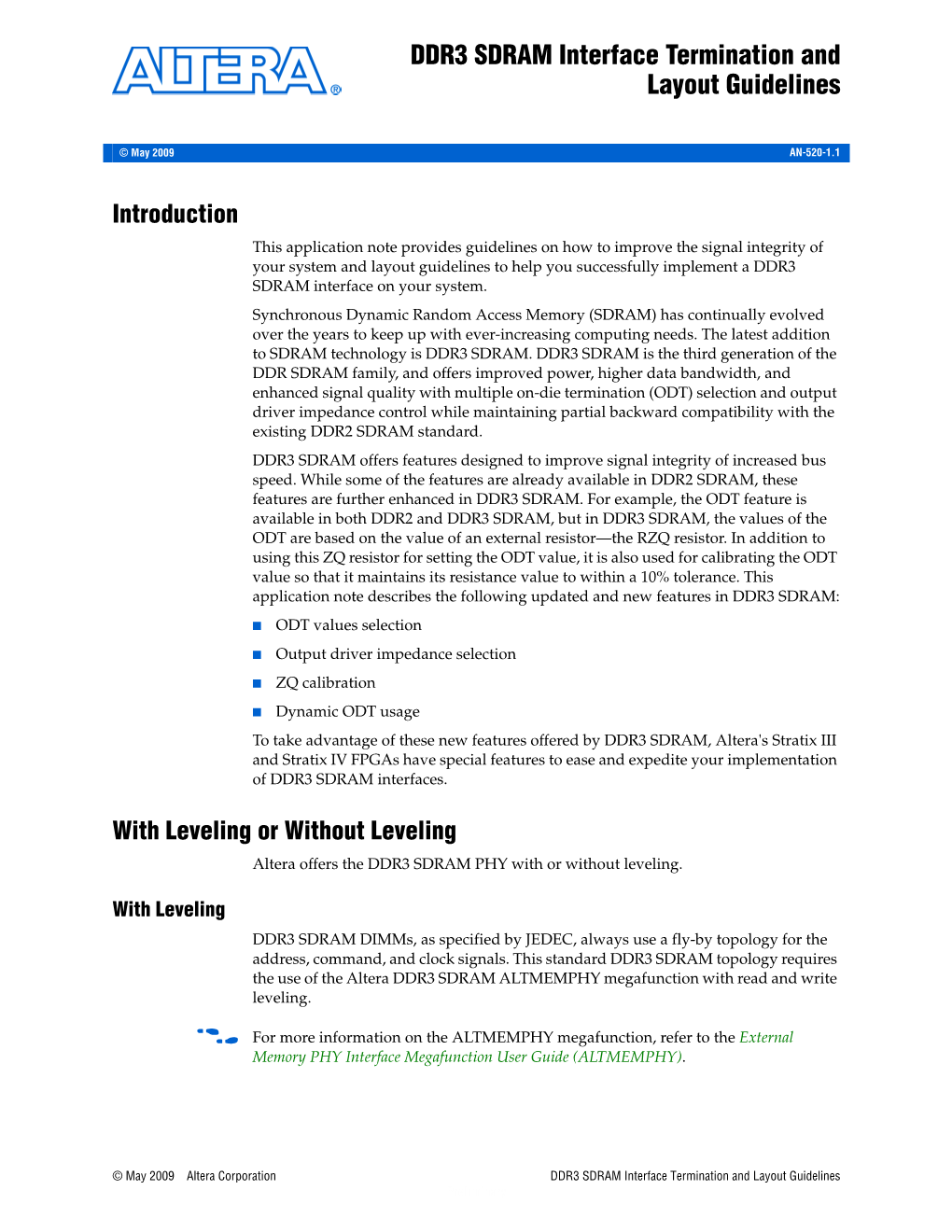
An520 DDR3 SDRAM Memory Interface Termination And Layout Guidelines
 www.scribd.com
an520 DDR3 SDRAM Memory Interface Termination and Layout Guidelines ...
The Best High Speed Board Design Guidelines | NWES Blog
 www.nwengineeringllc.com
The Best High Speed Board Design Guidelines | NWES Blog
High-Speed PCB Design Guidelines
 circuits-diy.com
High-Speed PCB Design Guidelines
Pcb Design Guidelines Mechanical Layer Eurocircuits Eurocircuits Images
 www.tpsearchtool.com
Pcb Design Guidelines Mechanical Layer Eurocircuits Eurocircuits Images
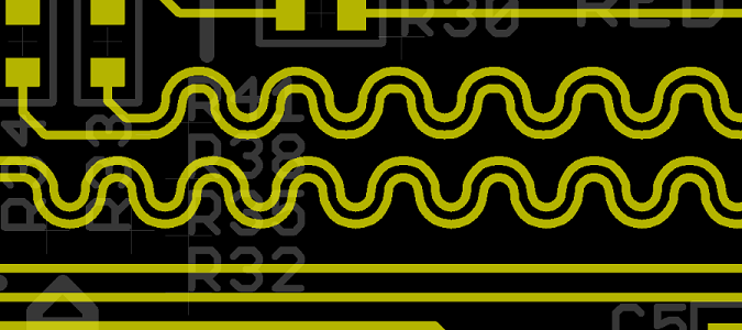
Ddr3 Pcb Layout Rules - PCBSky
 www.pcbsky.com
Ddr3 pcb layout rules - PCBSky
PCB Design Rules And Tips
 www.6pcb.com
PCB Design Rules and Tips
Video: IMX6 DDR3 Memory Layout – Preliminary Connections - IMX6 Rex
 www.imx6rex.com
Video: iMX6 DDR3 memory layout – Preliminary connections - iMX6 Rex ...
High Speed Pcb Layout Guidelines - Design Talk
 design.udlvirtual.edu.pe
High Speed Pcb Layout Guidelines - Design Talk
PCB Layout Guidelines For High Speed Applications - HardwareBee
 hardwarebee.com
PCB Layout Guidelines For High Speed Applications - HardwareBee
Pcb Routing Guidelines - Design Talk
 design.udlvirtual.edu.pe
Pcb Routing Guidelines - Design Talk
PCB Layout Services
 www.hytek-ed.com
PCB Layout Services
DDR3 SDRAM Memory Interface Termination And Layout Guidelines - DocsLib
 docslib.org
DDR3 SDRAM Memory Interface Termination and Layout Guidelines - DocsLib
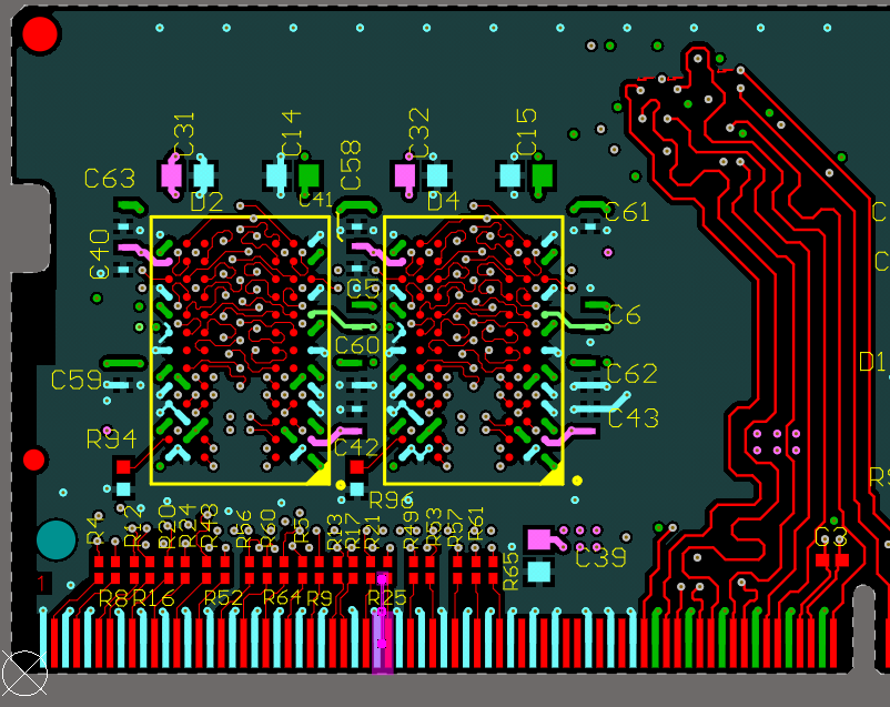
S6-DDR3: PCB Layout Considerations
s6-DDR3: PCB Layout Considerations
Alpha PCB - PCB Design Gallery
 alphapcbdesigns.com
Alpha PCB - PCB Design Gallery
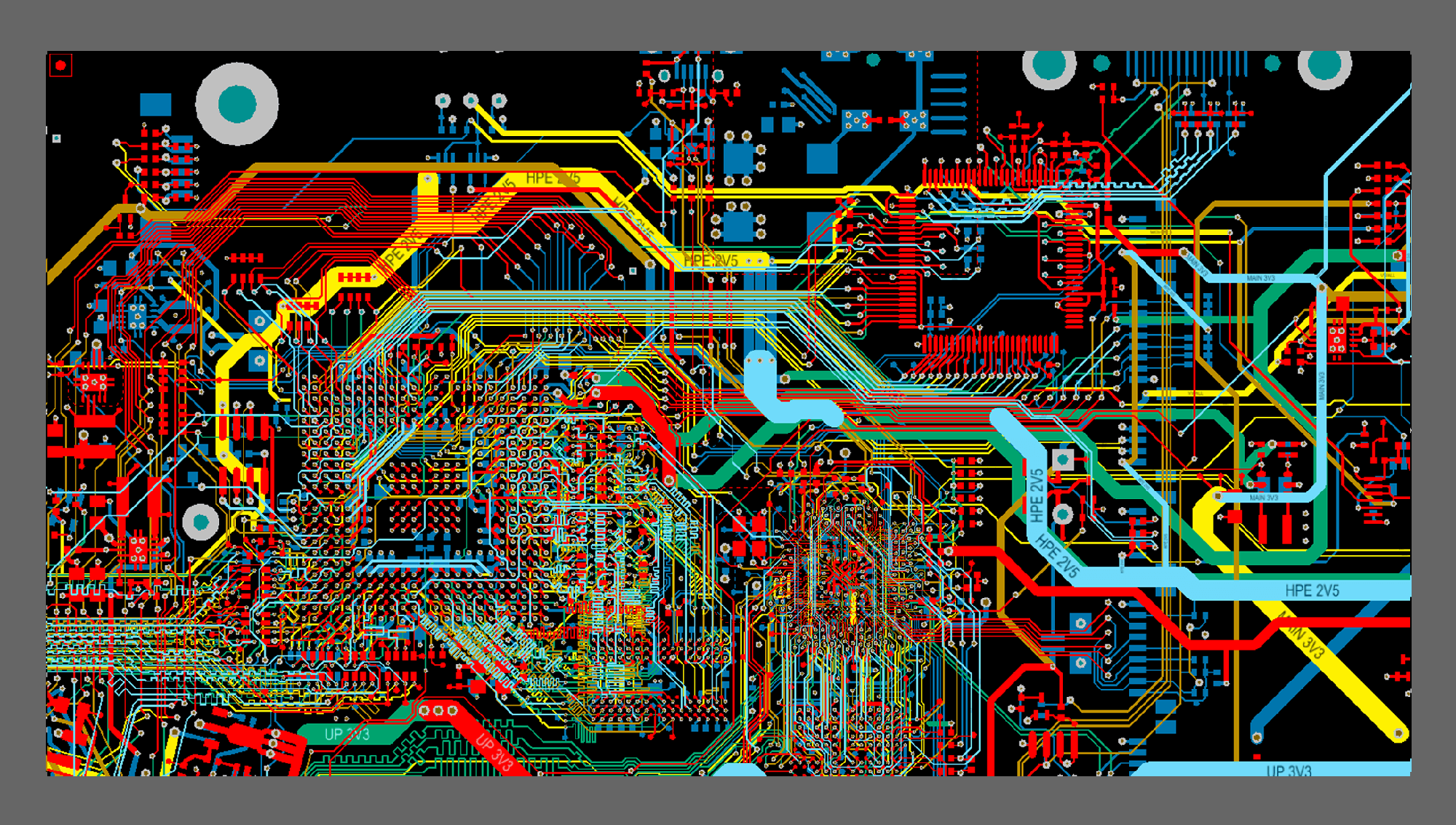
Main Design Guidelines & Layout Rules On High Speed PCB
 www.integrasources.com
Main Design Guidelines & Layout Rules on High Speed PCB
Main Design Guidelines & Layout Rules On High Speed PCB
 www.integrasources.com
Main Design Guidelines & Layout Rules on High Speed PCB
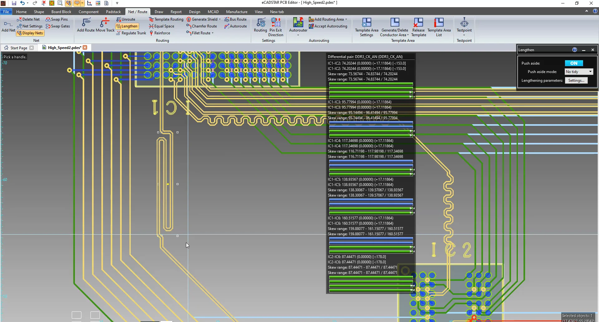
High-Speed Design | PCB | Video Library | ECADSTAR
 www.ecadstar.com
High-Speed Design | PCB | Video Library | eCADSTAR
Kintex-7 FPGA KC705 Evaluation Kit - AMD / Xilinx | Mouser
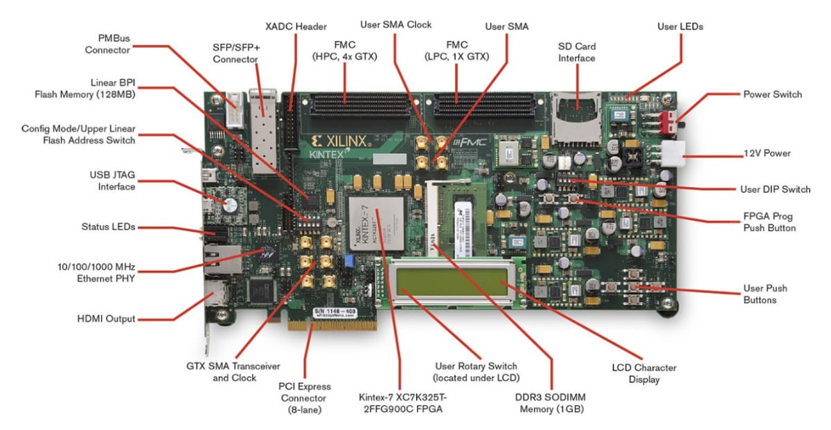 www.mouser.in
Kintex-7 FPGA KC705 Evaluation Kit - AMD / Xilinx | Mouser
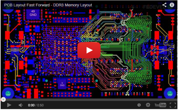
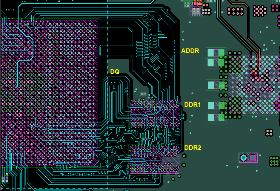
DDR3 Layout Vs Memory Chip Fitting
 www.fedevel.com
DDR3 layout vs Memory chip fitting
(PDF) Board Design Layout Guidelines; External Memory … · Introduce The
 dokumen.tips
(PDF) Board Design Layout Guidelines; External Memory … · introduce the ...
The Best High Speed Board Design Guidelines | NWES Blog
 www.nwengineeringllc.com
The Best High Speed Board Design Guidelines | NWES Blog
AMD Xilinx Spartan-6 FPGA DDR3 Signal Integrity Analysis And PCB Layout
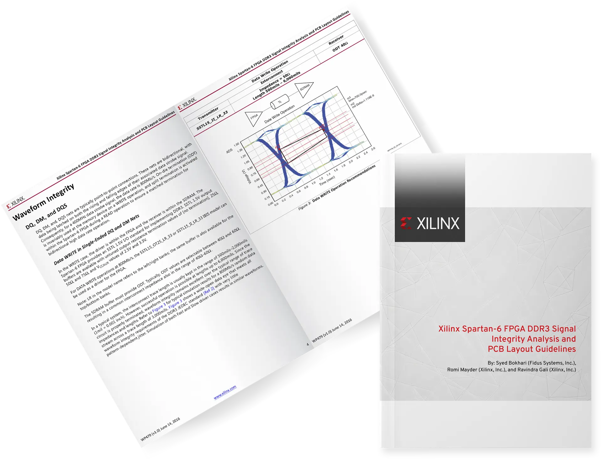 info.fidus.com
AMD Xilinx Spartan-6 FPGA DDR3 Signal Integrity Analysis and PCB Layout ...
Pcb layout guidelines for high speed applications. high-speed pcb design guidelines. Amd xilinx spartan-6 fpga ddr3 signal integrity analysis and pcb layout ...